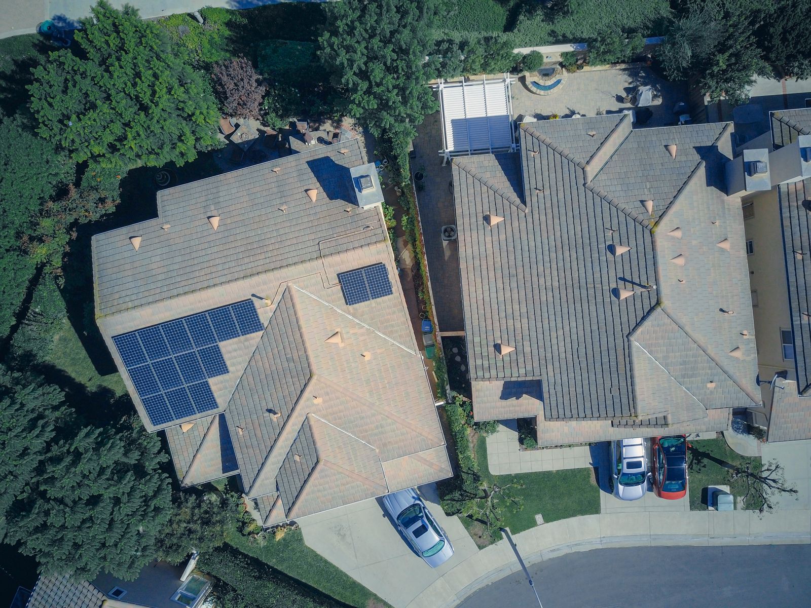
The dark cells on a suburban roof begin much earlier than the cell line or module factory. High-purity polysilicon is melted, an oriented seed crystal touches the surface, and a cylindrical single crystal is pulled upward while the seed and crucible rotate. After cooling, the ingot is cropped, shaped and sliced into wafers; only then are those wafers processed into cells and connected into a panel.
That sequence matters because a solar cell is not cut directly from an ingot, and a finished panel is not one unbroken crystal. The U.S. Department of Energy’s manufacturing overview separates the stages clearly: ingot and wafer production, cell fabrication, then module assembly. The molten centre of that chain is Czochralski growth, a slow and tightly controlled process whose complete cycle can occupy roughly two days.
One crystal, then one wafer
Pure silicon melts at 1,414 degrees Celsius. Just above that point it becomes a reflective liquid, while below it the atoms settle into the diamond-cubic lattice that gives crystalline silicon its electronic properties. The goal of the puller is to solidify a large charge without allowing the useful crystal body to break into differently oriented grains.
The seed crystal provides the template. As silicon atoms freeze at the surface of the rising seed, they follow its crystallographic orientation, so the useful body of the ingot becomes one continuous single crystal, apart from defects the process is designed to suppress. An AI-assisted Nature Research Intelligence summary describes the Czochralski technique as the cornerstone of high-purity single-crystal production and emphasises the linked roles of convection, heat transfer, dopant transport and thermal gradients.
The method began as a way to measure how quickly metals crystallised, not as a plan for producing solar wafers. A historical account dedicated to Jan Czochralski dates the discovery to 1916 and notes that the first description appeared in 1918; the familiar pen-and-molten-tin story is presented as the accident that prompted his controlled experiments. The industrial version that followed is vastly larger, but the central idea remains recognisable: touch a seed to a melt and withdraw it slowly enough for a crystal to grow.
Inside the puller
A photovoltaic Czochralski puller is a sealed furnace built around a quartz crucible, graphite heating components and a controlled argon atmosphere. Polysilicon chunks are melted, dopants are added as required, and the seed is lowered until it contacts the surface. Operators then form a narrow neck, widen the crystal into a shoulder, hold a nearly constant diameter through the body and taper it into a tail.
The crystal and crucible normally rotate at different speeds, often in opposite directions, while the pull rate and heater power are adjusted continuously. A photovoltaic reference chapter by Peter Dold, reproduced by ScienceDirect, lists typical PV ingots up to two metres long, standard body-growth rates around 1.0 to 1.3 millimetres per minute, and separate rotation ranges for the ingot and crucible. These are operating ranges, not a single recipe for every furnace.
The same chapter puts the timing in useful perspective. Crystallising the body of a two-metre ingot can take about 25 to 35 hours, while the complete cycle can take 50 to 60 hours once melting, necking, shoulder formation, tailing and the other process stages are included. The often-repeated “roughly two days” figure therefore describes a full industrial cycle reasonably well, but it should not be assigned to every 700-millimetre ingot as though the duration were fixed.
The boundary that decides the crystal
Much of the process is decided at the solid-liquid interface, the moving boundary where the melt becomes crystal. Heat must leave quickly enough for solidification to continue, but not so unevenly that the diameter drifts, thermal stress rises or dislocations spread. Cameras, load measurements and control systems watch the process because a loss of single crystallinity can force operators to remelt part of the run or sacrifice yield.
Flow inside the crucible is equally important. Rotation produces large circulation patterns, temperature differences drive buoyancy, and surface-tension effects create Marangoni flow near the exposed melt. These motions redistribute heat, dopants and oxygen, so changing a rotation rate or heater arrangement can alter the material that later reaches the wafer line.
Oxygen has to be controlled, not simply banished
The quartz crucible is silicon dioxide, and hot liquid silicon slowly reacts with it. Some oxygen enters the melt and a large share leaves the surface as silicon monoxide carried away by argon, while some remains in the growing crystal. The engineering problem is not captured by saying oxygen is simply a villain: certain oxygen-related defects and nonuniform concentrations can hurt performance, so manufacturers control how oxygen enters, moves through and leaves the melt.
A 2024 study from Taiwan’s National Chin-Yi University of Technology modelled a 200-millimetre-diameter, 700-millimetre-long ingot in a 20-inch crucible containing about 250 kilograms of silicon. The researchers found that crucible rotation changed oxygen concentration near the wall, with consequences for wafer mechanical and electrical properties. That study supports the geometry and rotation claim, but it does not establish a two-day pull time for that particular ingot.
A separate paper from the same university investigated a redesigned heater that reduced oxygen concentration in simulations and validation tests. Another Norway-Germany collaboration found that quartz-sand quality, particle size and manufacturing history influence crucible uniformity and properties. Together, these studies show why furnace design and crucible quality matter without reducing the entire problem to one impurity number.
The stakes become clearer as cell efficiencies climb. In April 2026, Trina Solar reported a certified 28.0% result for a TOPCon-compatible hybrid back-contact cell and said it was the first large-area 210R crystalline-silicon cell to cross the 28% threshold. Achievements at that level depend on the whole manufacturing chain, including the electrical quality and uniformity of the wafer entering the cell process.
From ingot to wafer to cell to module
After the crystal cools, the neck, shoulder and tail are removed, and the cylindrical body is machined into a shape that packs efficiently into rectangular modules. Cropping and squaring create offcuts, but clean offcuts remain valuable solar-grade silicon. A July 2026 update to the IEA-PVPS life-cycle inventory quotes Matthias Stucki of IEA-PVPS Task 12, who explains that scrap from cropping and squaring monocrystalline ingots can be returned to crystal growth, turning part of the waste stream into a closed loop.
Diamond-coated wires then slice the shaped ingot into wafers only a fraction of a millimetre thick. The cuts create kerf, the silicon lost as fine particles, but the same IEA-PVPS update reports that thinner diamond wires have reduced the amount lost per wafer. That is a different material problem from the clean offcuts generated during cropping and squaring, which are much easier to reintroduce.
The wafer still is not a solar cell. It must be textured, doped or otherwise junction-formed, passivated, coated and metallised so it can absorb light and collect electrical current. Only after many finished cells are electrically connected and laminated between protective materials does the familiar glass-fronted module emerge.
Two days of growth, decades of current
Once installed, a module is expected to operate for decades, but the electrical path through each monocrystalline cell still depends on a lattice established during the pull. The seed’s orientation is inherited by the ingot, the wafer inherits it from the ingot, and the cell inherits the wafer’s material quality. The panel itself, however, is an assembly of many cells rather than a single crystal stretched across the roof.
The scale of the route is difficult to overstate. The 2026 International Technology Roadmap for Photovoltaics says crystalline silicon accounts for roughly 98% of global PV production, monocrystalline Czochralski wafers remain standard, n-type wafers have reached about 82%, and TOPCon led in 2025. The roadmap expects tandem silicon cells to enter mass production after 2027, suggesting that future absorber stacks are likely to build on the silicon platform rather than make crystal growth irrelevant overnight.
Global deployment is growing just as quickly. The official IEA-PVPS Snapshot of Global PV Markets 2026 says installed photovoltaic capacity reached nearly 3 TW in 2025, up from 2.3 TW a year earlier. Because thin-film technologies still occupy part of the market, it would be wrong to say every watt began in a Czochralski crucible, but most of today’s production follows the crystalline-silicon route.
A bright pool, a slow-moving crystal
Through a furnace viewport, the hot zone appears bright while the melt remains reflective and restless beneath the rising crystal. The body advances at around a millimetre per minute, turning steadily as heat, flow and diameter controls keep the interface stable. For long stretches, the machine seems to do little more than rotate and lift.
What leaves the chamber is not yet a cell and certainly not a panel. It is one continuous crystal that will be cropped, squared, sliced, chemically transformed, metallised, interconnected and laminated before it reaches a roof. The wonder of the process is sharper when the sequence is stated precisely: most rooftop monocrystalline cells begin as wafers cut from a crystal whose atomic order was copied from one small seed at the surface of molten silicon.