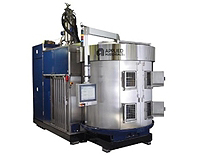
Applied Materials has released its Applied HCT MaxEdge wire saw, a new platform for slicing ingots into ultra-thin wafers that can help customers drive down the cost of manufacturing photovoltaic (PV) cells by up to $0.18 per watt.
Key technical advances, including an industry-first dual-wire management system, enable the MaxEdge system to deliver significantly higher throughput and load capacity than competitive systems, while requiring much less factory floor space and fewer operators for equivalent megawatt output.
By making thinner wafers, PV cell manufacturers can reduce the amount of silicon per wafer and lower the cost-per-watt of solar electricity.
To produce thinner wafers, traditional wire saws must reduce the ingot length (load) and the cutting speed. The uniquely designed MaxEdge system delivers ultra-thin wafers without sacrificing throughput by enabling larger loads and using thinner wires at higher cutting speeds.
"With the MaxEdge system we've boosted the wafer output and lowered the operating expenses of our industry-leading Applied HCT B5 system, making the best wire saw on the market even better," said Stefan Schneeberger, vice president and general manager of Applied Materials' Precision Wafering Systems division.
"The MaxEdge system builds on a 25-year history of wire saw innovation and incorporates key feedback from our customers. Since the wafer is the most expensive component of crystalline silicon-based PV manufacturing flow, reducing wafer fabrication cost is critical to the goal of making solar energy competitive with grid power."